March 28, 2025
P-n junctions form the foundation for much of modern electronics, due to their highly nonlinear IV characteristics. Additionally, due to electron-hole pair production, p-n junctions exhibit a voltage response to incident light. In this report, the IV characteristics of a Germanium p-n junction was measured, and the relationship of the photovoltage to intensity of incident light was verified. Further, using semi-log methods, the carrier lengths and lifetimes of electrons and holes were estimated. Finally, also using semi-log methods, the quantity \(e/k_b\) was estimated to be \(10937 \pm 23\) V\(^{-1}\).
The p-n junction, commonly referred to as a diode, is a foundational component of modern electronics. In principle, an ideal diode allows current to flow in one direction through a circuit, but not another. Although p-n junctions are not ideal diodes, their highly nonlinear current voltage relationships closely approximate this property, enabling them for use in computational settings, specifically as components of transistors. Additionally, due to the IV relationships dependence on temperature and illumination, p-n junctions can be used as sensors, and are the fundamental building blocks in solar cell power generation.
Semiconductors are materials with a small band gap of around 1-3 eV between valence and conduction states of electrons, enabling a small amount of conduction at room temperature. In most electronics applications, semiconductors are doped with impurities. When doping introduces an extra electron, the semiconductor is called n-type, and when an extra spot in the valence shell for an electron is created, also referred to as a hole, the semiconductor is called p-type. As an example, Silicon, a semiconductor, could be doped with Phosphorus (on the order of \(10^{13}\) to \(10^{18}\) P atoms\(\cdot\)cm\(^{-3}\) to \(10^{22}\) Si atoms\(\cdot\)cm \(^{-3}\))\(^{[1]}\). Each Silicon atom has four valence electrons, and bonds with four other Silicon atoms to form an octet, such that each valence electron is in a bond. When Silicon is doped with Phosphorus, the Phosphorus atoms each randomly replace one Silicon atom, but end up leaving one valence electron unbonded, due to Phosphorus possessing five valence electrons. Since the valence band of pure Silicon is already filled, the added electron is free to conduct. In reality, the extra electron forms a bound state with the Phosphorus nucleus, but requires very little energy to be excited into conduction.
A p-n junction is formed by placing a p-type semiconductor in contact with an n-type semiconductor. What results is what is called a depletion region at the interface of the two types, due to the loosely bound electrons in the n-type semiconductor filling the empty valence spots on the p-type side, states which are at a much lower energy. As shown in figure 1n, the electrons leaving the n-type semiconductor leave behind an extra proton, and the filled holes in the p-type region add an extra negative charge. Thus, what results is a permanent charge imbalance, and a voltage between the p and n regions.
If a voltage difference is applied over the junction a current will flow. Figure 1b models the band structure of the junction as a function of space, where the difference in energy between the p and n regions is due to the ambient induced voltage from the depletion region. There are two processes that contribute to a voltage dependent current: the movement of electrons in the n-type conduction band to the p-type conduction band, and holes moving from the p-type valence band to the n-type valence band. In each case, the difference in energy that the carriers must traverse depends on the voltage applied across the junction. The probability that any one carrier will make a transition to another state is given by the fermi distribution function. At the temperatures dealt with in this experiment, the function can be approximated as:
\[f(E) = \frac{1}{e^{-\frac{E-\mu}{k_bT}}+1}\approx e^{-\frac{E-\mu}{k_bT}}\]
We take the probability of an electron making a transition from the n-type to p-type semiconductor (and vice versa for holes) to be proportional to the net current across the junction. After subtracting out the process by which an electron in the p-type region is thermally excited into the conduction band, and descends energetically into the n-type region conduction band, we get the following current voltage relationship, where \(J_s(T)\) represents the saturation current, and appears due to this subtraction:\(^{[2]}\)
\[I = J_s(T)(e^{-\frac{eV}{k_bT}}-1)\]
In this experiment, the photovoltaic effect was also investigated. If light of high enough energy is shined upon a semiconductor, electrons can be excited into the conduction band, creating a hole in the valence band at the same time. Keeping in mind the band diagram in Fig 1b, these excited electrons may diffuse towards the depletion region and into the n-type region, which is lower in energy, and thus more favorable. The same logic applies to holes in the reverse direction. The result is a further build up of charge between two sides of the junction, and thus an even larger voltage difference, called a photovoltage.\(^{[3]}\)
In this report, a Germanium p-n junction was investigated. First, the IV characteristics were measured, and shown to follow the relationship previously described. Next, the existence of the photovoltaic effect was verified, and a focused light beam was utilized to measure how far electrons and holes are able to diffuse within the junction as well as their lifetimes. Finally, using semi-log plot techniques, the IV curves of another diode were used to estimate the quantity \(e/k_b\), at several temperatures.
The IV characteristics of a Germanium planar diode were measured. The junction itself is mounted in an acrylic holder, such that the p and n regions are both exposed to the ambient light of the testing room. The holder itself has two possible connections over the junction: a direct connection through a BNC, which was used to measure the voltage across the junction with a Keithley 2110 Multimeter, and another that has two 300\(\Omega\) resistors in series to prevent large currents, which was used to gate the junction. A 1.5V battery and a variable potentiometer was used to gate the junction at varying voltages. In series with the potentiometer and the junction, the current was measured using another Keithley 2110 Multimeter.
Next, the behavior of the junction under illumination was investigated. First, the battery was taken out of the circuit, and the potentiometer was set to one resistance (R = 137.9\(\Omega\)). A small white LED was mounted at the same height as the planar junction, and driven by a 1Hz square wave from a function generator. The amplitude of the function generator signal was varied until the photovoltage over the junction was maximized. Finally, the photovoltage was recorded at multiple distances from the diode. A black piece of fabric was laid over the set up to ensure that no ambient light influenced the results. Driving the LED at 1Hz gave the junction enough time to respond to the on and off states, however, the value was still somewhat inconsistent. Thus, for each distance, upper and lower voltages were recorded over 10 cycles after which a mean change in voltage was calculated, with an associated statistical error.
A reliable calculation of these constants requires very precise focusing of light on the p-n junction. Thus, a focusing lens was placed between the junction and the LED, and moved until as tight a beam as possible could be made on the surface of the junction and the photovoltage signal was maximized. Then, a Mitutyo micrometer was used to adjust the perpendicular displacement of the diode with respect to the light beam in successive steps of 0.325 and 0.3 mm. This way the beam was able to scan across the p, the depletion, and finally the n region. The data collection and circuit were otherwise unchanged from the previous section.
Finally, the constant \(e/k_b\) was estimated at several temperatures. To gain control over temperature, a 2N3053 NPN power transistor, immersed in mineral oil, was used instead of the Germanium diode from before. The 2N3053 was essentially made to be a p-n junction by shorting the collector and base, and measuring the current and voltage between the base and emitter. Four IV curves were recorded at 77K, 274K, 295K, and 373K. The 77K measurement was done using liquid nitrogen, and was the only measurement to be done with a different power transistor than the others, which was exposed directly to the liquid nitrogen instead of being submerged in oil. The 274K measurement was done in ice water, and the 373K was done on a hot plate.
The collected data was processed using python and the scipy.optimize package. Extraction of fundamental constants in the last two experiments was done by taking the log of one of the parameters, and fitting the data to a linear function using scipy. In all cases, the error of the Keithley multimeters was found from a standard table published by the company itself\(^{[5]}\). Given that sometimes the devices seemed to be less accurate than the company claimed, one half of the last reliable digit of each measurement was added in quadrature to this value. This was considered the systematic error. The error of fundamental constants calculated is given as one value due to the fact that the error given to the scipy regression model was the statistical and systematic error added in quadrature. The regression then calculated an uncertainty in the constants based upon both quantities.
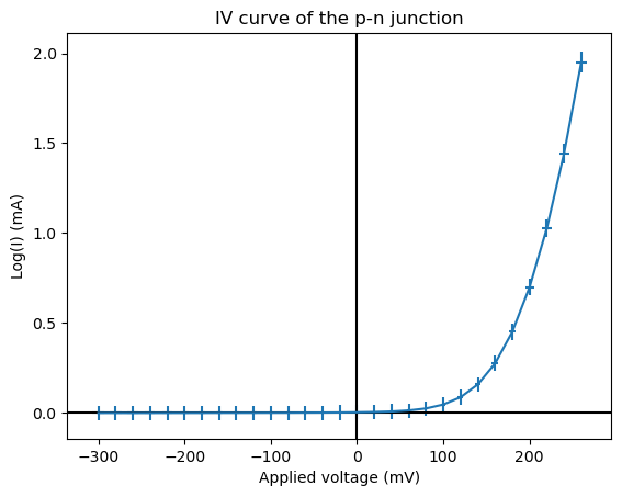
First, the IV curve of the Germanium junction was characterized.
The results are plotted in Figure 2. Qualitatively, the curve matches the common diode equation described earlier and in [2]. From the graph we can estimate the saturation current to be around \(J_s(T) \approx -0.0034\) mA. While the magnitude of this value is actually very large compared to existing literature, this is likely due to the fact that these measurements were not taken in a dark environment. A forward voltage is estimated to be around 150 to 200mV.
Next, the response of the junction to illumination at different distances was investigated.
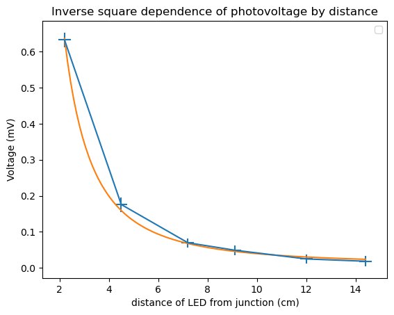
As described before, illumination of the p-n junction should result in the diffusion of electrons and holes across the depletion region, causing a photovoltage across the junction. Since the amount of light incident on the junction will be directly proportional to the number of electron hole pairs created, the intensity of the light should directly correspond to the photovoltage measured. Since light intensity is proportional to the inverse square of the distance from the source, the photovoltage should also have this same dependence, which can clearly be seen in Figure 3. Using regression, the data was fit to an inverse square function, and found to have a reduced chi squared of about \(X^2_{red} \approx 1.153\).
By changing the horizontal position of the junction and focusing the LED, the diffusion lengths and lifetimes of both electrons and holes were calculated.
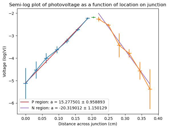
As described by Goucher et al.\(^{[6]}\), the diffusion of carriers, some distance x from the depletion region of the device, to the other side of the junction (the cause of the photovoltage), is proportional to exp\((-x/L)\). Where L is the diffusion length of the carrier, D is the diffusion constant, and tau is the carrier lifetime. Given this relationship, we should expect the photovoltage to increase exponentially as we approach the depletion region of the junction, as more and more carriers will move across the junction for smaller x. We also notice that the slopes of the P and N regions–on the left and right respectively in Figure 4–are different, implying that the lengths and lifetimes of electrons and holes are different. In fact, the diffusion constants are different as well, \(D_n = 43\) cm\(^2\cdot s^{-1}\) \(D_p = 92\) cm\(^2\cdot s^{-1}\). To extract the diffusion lengths, we format the data in a semi-log plot, noticing that:
\[V_{ph} \propto e^{-\frac{x}{L}}\implies ln(V_{ph}) \propto -\frac{x}{L}\]
Thus, the magnitude of the slope of the semi-log plot should be \(1/L\). Fitting to this data with a linear regression on the right and left sides of the junction, and solving for the lifetimes using the equation \(L = \sqrt{D\tau}\), the following values were obtained:. \[\begin{array}{|c|c|c|} \hline & \textbf{P region} & \textbf{N region} \\ \hline\hline \text{Exp}& L_p = 0.655 \pm 0.041 \text{mm}& L_n = 0.492 \pm 0.028 \text{mm} \\ \hline & \tau_p = 46.6 \pm 5.8\mu s & \tau_n = 56.3 \pm 6.4 \mu s\\ \hline \text{Acc}& L_p = 0.7\text{mm} & L_n = 0.5\text{mm} \\ \hline & \tau_p = 52 \mu s & \tau_n = 56 \mu s\\ \hline \end{array}\]
The above table shows the experimental values were all nearly within a standard deviation of the accepted result.
One possible explanation for the deviation from the accepted values may be that the errors in this experiment were too high. When converting data to a log plot, the error of each data point also had to be propagated, introducing a \(1/V_i\) to the ith error. Since the data furthest from the junction had such a small photovoltage, this meant that the propagated error was very high, possibly throwing off the regression.
Finally, the quantity \(e/k_b\) was calculated from several IV curves at different temperatures.
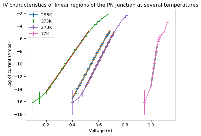
Figure 5 shows a semi-log plot of the IV curves of the two 2N3053 power transistors at various temperatures. A semi-log plot is used for the same reason as in the previous section: the diode equation is exponential.
\[I\approx J\cdot e^{\frac{-eV}{k_bT}} \implies Ln(I) \approx Ln(J) - \frac{eV}{k_bT}\]
Given this fact, the slope of the semi-log plot of the IV curves should give us \(e/k_bT\). The slopes were again estimated using linear regression, and then were multiplied by the T of each curve to obtain an estimate for \(e/k_b\), shown in the table below.
\[\begin{array}{|c|c|} \hline \textbf{Temperature} & \textbf{$e/k_b$} \\ \hline\hline 77 K& 11028 \pm 7 \\ \hline 273K & 11115 \pm 6 \\ \hline 295K & 11056 \pm 10 \\ \hline 373K & 10574 \pm 19\\ \hline \end{array}\]
Averaging the four values together, we obtain a value of \(e/k_b = 10937 \pm 23\). From this we can see that our estimate for \(e/k_b\) varies from the accepted value of \(11064.9 \pm 0.6\) 0 by 5.75\(\%\). All valued are reported in units of inverse volts.
As can be seen in Figure 4, the IV curves of transistors diverged from the expected exponential relationship for high and low values of voltage. In reality, the diode equation breaks down at extremes due to other effects contributing to the amount of current flowing, such as the recombination current, or surface effects\(^{[7]}\). In this study, the linear region of the semi-log plot of the IV curve was simply found by visual inspection (the linear region being where the junction follows the diode equation most closely).
The fit for this plot suffered from the same issue of extremely high errors for low current measurements as in the previous experiment, which may have driven up the difference from the true value of e/k. The estimates for e/k are consistently lower than expected, however, suggesting the temperature could have been consistently lower than the true value. What we believe is more likely is that surface effects, which act to add an extra parameter m, called the ideality factor, have become important in this case, which would account for a consistent deviation from the expected value, though Inman et al. argues that power transistors should not exhibit these defects. Of course there is also the possibility that something else in the circuit also has a nonlinear current voltage relationship, affecting the results.
The main aim of this project was to investigate the properties of p-n junctions. First, a typical IV curve was measured for a planar Germanium junction, which qualitatively matched the predicted relationship. Next, the Germanium junction was illuminated with a white LED, which varied in distance from the junction. A clear inverse square relationship measured to high statistical confidence, as was expected. Using the same LED, a focused beam of light was scanned across the p and n regions in order to calculate the diffusion lengths and lifetimes of electrons and holes from each of those regions, respectively. Finally, using a power transistor in controlled temperature environments, the constant e/k was calculated from the slope of the semi-log plot of the IV curve. Overall, this study showcased the usefulness and complexity of the p-n junction. Whether being used for energy generation in photovoltaic cells, or for calculations of fundamental constants, the p-n junction is foundational to modern electronics. In future iterations of the study, beyond improvement of data acquisition techniques, we would hope to investigate the photovoltaic effects dependence on frequency of incident light. By varying the frequency, the exact value of the band gap of the doped semiconductor could theoretically be measured.